Supports Embedded DisplayPort (eDP) Specification version 1.2.
Support 4 Main Link Lanes at either 1.62Gb/s or 2.7Gb/s link rate
Supports input color depth 6/8/10-bit per pixel in RGB format
Support VESA and CEA timing standards up to QSXGA 2560x2048 @ 60Hz or WQXGA 2560 x 1600 @ 60Hz for 2D, and Full HD 1920x1080 @120Hz for 3D(L/R eye frame at 60Hz each), with 10 bit graphic color depth
Support eDP Authentication: Alternative Scramble Seed Reset (ASSR) and Alternative Framing
Support Single Port, Dual Port and Quad port LVDS output interface with 6/8/10-bit color depth up to 400MHz pixel rate
Support both OpenLDI (or JEIDA), SPWG (or VESA) and non-JEITA (10-bit only) bit mapping for LVDS application
Flexible LVDS output pins swapping
2 channel IIS/ S/PDIF audio output
Support Dynamic Backlight luminance Control by the command through AUX channel, or through the interface of PWM in/out and Backlight Brightness Control (OSD display)
Support PWM bypass through and on-chip PWM generation (range 30~100%)Black panel during invalid input
Support Panel selection function with external hardware configuration
Initiated and controlled by firmware which is loaded from External BOOT ROM automatically upon power up.
BOOT ROM data updated through I2C bus or AUX Channel
Support dynamic refresh rate (DDR) switching
Supports Enhanced Framing Mode
3 work modes: connect 27MHz crystal, inject 27MHz or 14.318MHz clock
Programmable LCD panel power sequence
Hot Plug Detection
Support chip power down by GPIO pin
Support power management mechanism through AUX Channel
EMI reduction capability for DP input and LVDS output. Spread spectrum control is available for transmitting LVDS signal
Achieve bit error rate <10-9 for raw transport data per lane and symbol error rate <10-12 for control data
Low power consumption
Offered in a 128-pin TQFP package (14 x 14mm)
DESCRIBE
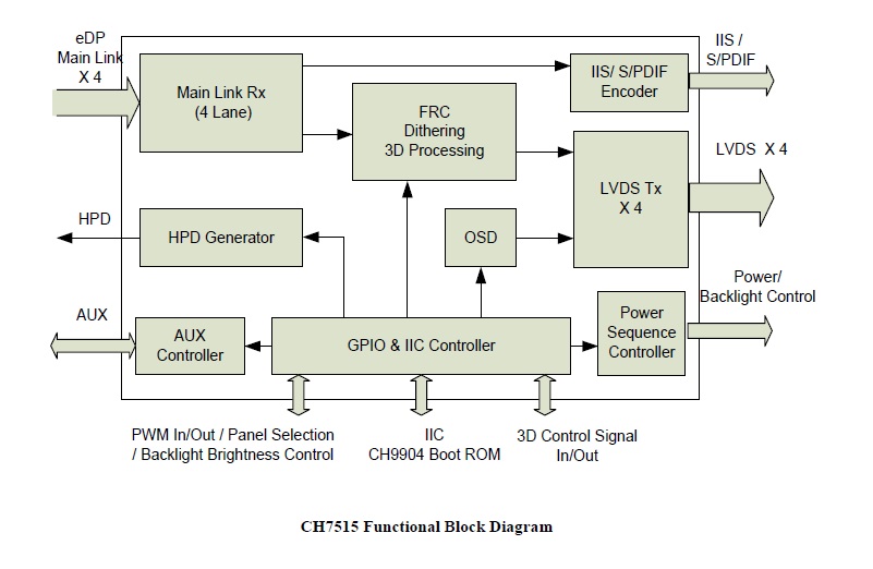
Chrontel's CH7515 is a low-cost, low-power semiconductor device that translates the Embedded DisplayPort signal to the LVDS in form of RGB/YCbCr 4:4:4/YCbCr 4:2:2. This innovative eDP receiver with integrated 4 channel LVDS transmitters is specially designed to target the All-In-One PC and the notebook market segments. Leveraging the DisplayPort's unique source/sink "Link Training" routine, the CH7515 is capable of instantly bring up the video display to the LCD when the initialization process is completed between CH7515 and the graphic chip.
The CH7515 is designed to meet the Embedded DisplayPort Specification version 1.2. The 4 eDP Main Link Lanes receiver supports input with data rate running at either 1.62Gb/s or 2.7Gb/s, and can accept digital RGB signal for LVDS output up to QSXGA 2560x2048@60Hz. With advanced 3D processing module integrated, The CH7515 can support up to 1920x1080@120Hz 3D display mode, with programmable emitter control signal and 3D LCD panel's backlight control signal output.
The Backlight Enable control and the PWM are the two kinds of backlight control functions designed in the CH7515 Panel power control module. The brightness control commands sent through AUX Channel can be dynamically translated by CH7515 and converted into LCD backlight control signal. Alternatively, the brightness control commands can be input from the PWM in and GOIO pin of Backlight Brightness Control. The CH7515 will save the last setting of brightness level into the external BOOT ROM and restore it upon power up. The CH7515 can dynamically adjust backlight brightness according to video stream to save power consumption and it supports OSD display in this way.
The CH7515 will immediately convert the Embedded DisplayPort signal to LVDS output after DisplayPort Link Training is completed. This feature can be achieved by loading the panel's EDID and the CH7515's configuration settings in the serial external BOOT ROM connected to the CH7515. During system power-up and upon completion of the DisplayPort Link Training through AUX Channel, CH7515 will generate LVDS signal according to the panel power-up timing sequencing stored in the external BOOT ROM.
An advanced Power Management Unit (PMU) is incorporated in CH7515, which is specially designed to reduce power consumption in normal operation.
Founded in 1986, Chrontel develops and markets mixed-signal integrated circuits. The company is a leading provider of display interface IC's for personal computers, portable media players & smartphones. Interfacing to different computing platform standards including TV, HDTV, LCD, ...